Abstract
In this article we present a reconfigurable instrumentation architecture that combines the modular composability of traditional instruments with the size and cost advantages of integrated dedicated controllers. Such instrumentation can be specified by a declarative configuration file written in terms of logical instruments — virtualized instrument functions that expose standardized signal ports and configurable parameters while hiding internal implementation. A compiler translates this file into complete physical hardware within minutes. Because the configuration vocabulary is finite and every file passes through compiler validation, large language models can generate configurations safely: the compiler acts as a non-bypassable barrier between AI output and hardware. The workflow is validated through an impedance measurement experiment.
1. Introduction
In modern experimental physics, a unified methodology has emerged: virtually all quantities of interest — temperature, light intensity, displacement, magnetic field, chemical concentration — are converted into electrical signals and then processed by digital processors. This common pathway, from physical quantity to electrical signal to digital data, is what allows a single measurement platform to serve radically different experiments. Here we propose a six-layer reference model that decomposes this methodology along the direction of signal flow, providing the precise vocabulary that the rest of the paper relies on.
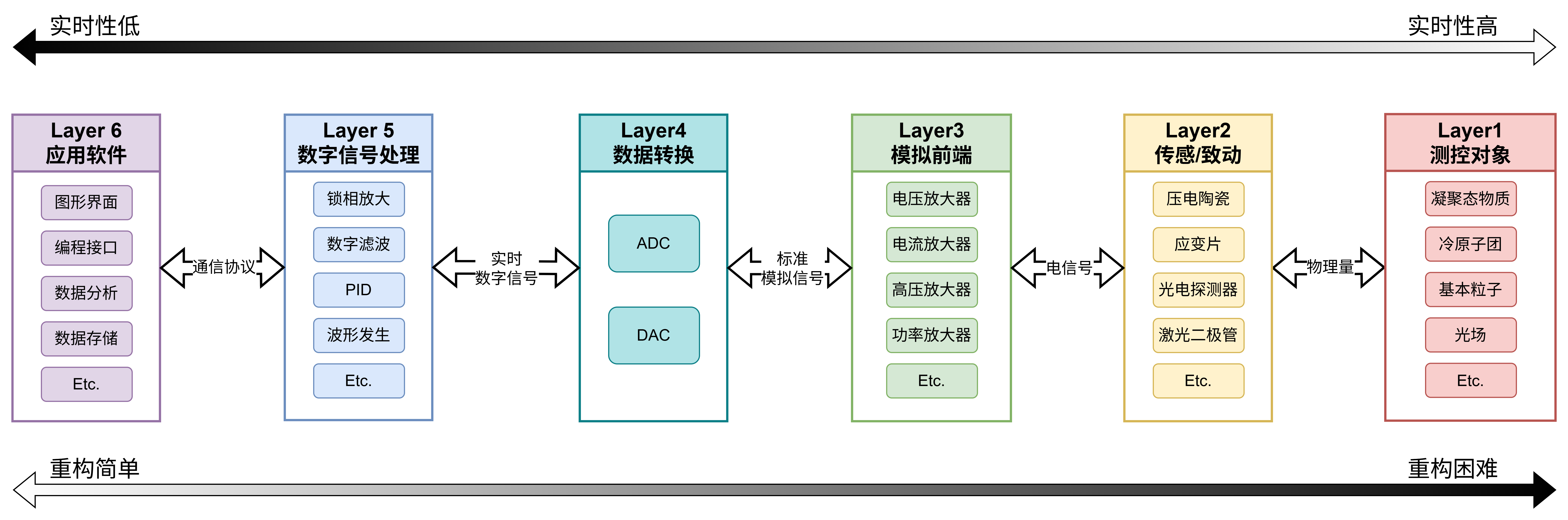
1.1 The six-layer reference model
We decompose a typical measurement system into six layers, numbered in the direction of signal flow from the physical world toward the user, as shown in Figure 1.
Layer 1 — Physical system under measurement or control. The physical object being studied or manipulated — condensed matter samples, cold atom clouds, optical fields, elementary particles, and so on.
Layer 2 — Sensors and actuators. The transducers that convert between physical quantities and electrical signals. Sensors (thermocouples, photodiodes, strain gauges) transform physical quantities into electrical signals; actuators (piezoelectric ceramics, laser diodes, resistive heaters) transform electrical signals into physical actions.
Layer 3 — Analog front-end and signal conditioning. Input front-end circuits amplify, filter, isolate, offset, and impedance-match raw voltage, current, or charge signals, bringing them into standardized ranges such as ±10 V. Typical input modules include low-noise voltage preamplifiers and transimpedance amplifiers. Output front-end circuits provide drive amplification and power delivery — high-voltage drivers for piezoelectric actuators, voltage-controlled current sources, and the like.
Layer 4 — Data conversion. Analog-to-digital converters (ADCs) discretize conditioned analog signals into digital sample streams; digital-to-analog converters (DACs) reconstruct analog signals from digital streams. This layer establishes a clear physical boundary between the analog and digital domains, introducing sampling rate, quantization bit depth, and conversion latency.
Layer 5 — Digital signal processing. The hard-real-time digital processing layer that executes all algorithms requiring deterministic timing. Implementation may use FPGAs, DSPs, or other deterministic processors. Typical tasks include waveform generation, waveform recording, lock-in amplification, digital filtering, PID control, pulse counting, and timing control.
Layer 6 — Application software. The non-real-time software layer running on a host computer, comprising device drivers, a graphical user interface (GUI), and data processing and storage modules. The user observes results, issues commands, writes instrument definitions, and triggers compilation from this layer.
1.2 Functional blocks
A functional block is defined as the smallest reusable functional unit residing at a specific layer — for example, an analog front-end circuit at L3 (a voltage amplifier or transimpedance amplifier), a digital signal processing IP core at L5 (a lock-in demodulation core or a waveform capture core), or a device driver or software API at L6 (a Python instrument interface or a GUI control panel). A functional block performs exactly one well-defined function within its layer. It is the atomic building block of all instrument functionality.
1.3 Inter-layer signals
Each boundary between adjacent layers carries a distinct category of signal:
- L1 - L2: Physical quantities. Light intensity, temperature, pressure, displacement, and so on.
- L2 - L3: Non-standard electrical signals. Sensors produce low-level voltages (millivolt range), weak currents (microampere to nanoampere range), or charge packets. Actuators may require large voltages, high power, or constant-current drive.
- L3 - L4: Standard analog voltages and currents. After conditioning, signals conform to standard ranges such as ±10 V, 0–5 V single-ended, or 4–20 mA current loops.
- L4 - L5: Real-time digital signal streams. ADCs output parallel or high-speed serial (LVDS, SPI) binary data, accompanied by a sampling clock and synchronization flags. In the DAC direction, the same format is received. At this boundary, signals have fully entered the discrete-time, discrete-amplitude digital domain.
- L5 - L6: Device communication protocols. Measurement results, configuration commands, and status information are exchanged over general-purpose digital protocols (USB, Ethernet, memory-mapped PCIe interfaces, register maps). This link does not require hard real-time guarantees and tolerates operating-system-level non-deterministic latency.
1.4 The trade-off between response time and design difficulty
The six-layer model exhibits a fundamental trade-off in measurement system design: closer proximity to the physical world yields shorter response times, but requires longer design cycles.
Response time increases from L1 to L6. L3 analog circuits can achieve bandwidths up to 100 GHz, yielding to ps-level response time; L5 FPGA processing introduces latencies on the order of 10–100 ns; L6 software operates at millisecond timescales. Design difficulty follows the opposite gradient, decreasing from L1 to L6. Designing and fabricating an L3 analog front-end board takes weeks per iteration; L5 FPGA programming takes hours per compile cycle; L6 software can be modified and tested in minutes.
Because both response time and design difficulty are tied to layer placement, the same function can be placed at different layers, trading response time for design convenience. PID feedback control, for instance, can be implemented at L3 (analog circuit, fastest, hardest to adjust), L5 (FPGA digital loop, intermediate), or L6 (software, slowest, easiest to reprogram). The choice of layer is a deliberate engineering decision that the six-layer model makes explicit.
2. The Logical Instrument
Layers L3 through L6 are the domain of the electronic instruments. The prevailing approaches to implementing these layers fall into two opposing paradigms: conventional commercial instruments, and integrated instrumentation. In §2.3 we introduce the concept of logical instruments, a virtualized abstraction that merges the merits of both.
2.1 Conventional commercial instruments
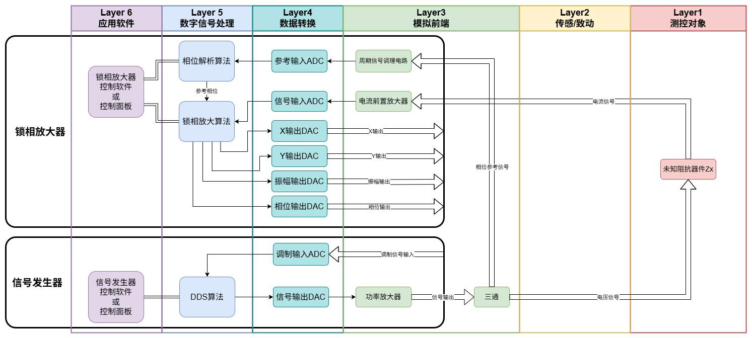
Take a lock-in amplifier as an example. Internally, a conventional commercial lock-in amplifier spans L3 through L6: an analog input stage (L3), ADCs and DACs (L4), a digital lock-in detection engine (L5), and a front-panel display with remote control interfaces (L6). All of these layers are permanently sealed inside the manufacturer's enclosure.
The critical limitation is that the internal L3–L6 connections are permanently fixed by the manufacturer. The user has no access to the signal nodes inside the instrument. When an experiment requires multiple instruments — say, a signal generator to drive a sample, a lock-in amplifier to detect the response, and an oscilloscope to monitor intermediate signals — these instruments can only be interconnected at the analog level (L3) through external BNC cables. The result is a physically large, complex system that often fills an entire equipment rack and whose internal signal paths are largely invisible to the user.
2.2 Integrated instrumentation
A natural response to the bulk and cost of conventional commercial instruments is to consolidate all signal processing onto a single FPGA, and to place the ADCs, DACs, and analog front-end circuits onto a single board alongside it. Such a system dramatically reduces size, cost, and power consumption, and is compact enough for embedded deployment.
The trade-off is generality. An integrated instrument is designed for a specific measurement task — its signal processing pipeline, its analog channels, and its software interface are all fixed at design time. It is a single-purpose device. To serve a different experiment, new hardware must be designed, laid out, and fabricated.
2.3 The logical instrument
Conventional commercial instruments (§2.1) are freely combinable and general-purpose, but large and expensive. Integrated instrumentation (§2.2) shrinks cost and volume substantially, but cannot be reconfigured and thus surrenders generality. The goal of this paper is to build on the integrated approach and, by introducing one core abstraction — the logical instrument — give it the same freedom of combination that conventional commercial instruments enjoy, while retaining its advantages in size and cost.
A logical instrument is a virtualized encapsulation of an instrument function. It is assembled from several cross-layer functional blocks (§1.2), but its internal implementation — the specific functional blocks and their interconnections — is completely hidden from the user. What is exposed are standardized signal ports and configurable parameters.
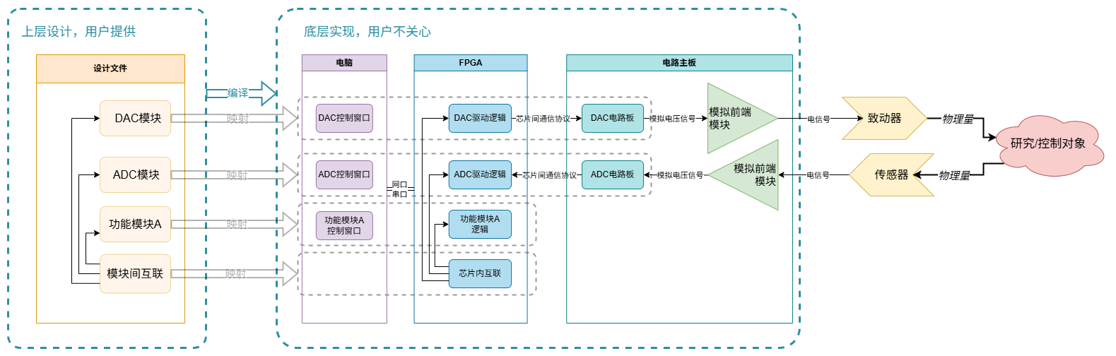
Logical instruments correspond roughly one-to-one with familiar instrument categories. Every conventional commercial instrument type — oscilloscope, lock-in amplifier, signal generator, PID controller — has a corresponding logical instrument. ADCs and DACs are also treated as independent logical instruments, rather than being embedded inside other instruments as they are in conventional commercial instruments.
Because logical instruments are fully decoupled from one another — communicating only through standardized signal ports — each can be versioned, upgraded, and maintained independently. A new revision of a lock-in amplifier block, for instance, can be deployed without touching the signal generator or PID controller alongside it.
Hence, the user can build with logical instruments just as they would with conventional instruments, but by editing a design description file. A compiler reads this file and generates the necessary executables — a workflow explained in detail in the next chapter.
3. Workflow: From Design Description to Physical Implementation
3.1 The design description file
A structured configuration file specifies the instrument system. The file uses a straightforward key-value format: it lists instrument instances by name, type, and parameters, and then declares port-to-port connections.
One such file completely defines the instrument system — which logical instruments are present, their parameters, and the full topology of signal flow between them.
The file is small (typically about 1 kB) and its format is intuitive. Any researcher familiar with instrument parameter sheets can read and write it directly. Meanwhile, its rigid vocabulary makes it suitable for automatic generation by a large language model (detailed in §4). Modifying the configuration file and recompiling transforms the same hardware platform into a completely different instrument system within minutes.
Example configuration file:
Instrument instances:
  - name: adc1,      type: AD402x
    output ports: [dataout]
  - name: dac1,      type: AD5791
    input ports: [datain]
  - name: osc1,      type: Oscilloscope
    parameters: n_channels=2
    input ports: [in0, in1]
  - name: dds1,      type: DDS
    output ports: [sigout]

Connections:
  adc1.dataout  →  osc1.in0
  dds1.sigout   →  dac1.datain
This example declares an ADC, a DAC, an oscilloscope, and a DDS signal source. It connects the ADC's data stream to channel 0 of the oscilloscope and routes the DDS output through the DAC. After compilation, the user obtains an instrument system capable of simultaneous waveform generation and data acquisition.
3.2 Currently supported logical instruments
The compiler ships with a library of instrument types covering signal processing functions and hardware interface blocks. The table below lists the currently supported logical instruments and their key specifications (typical values):
Signal processing instruments:
| Logical instrument | Key specifications |
|---|---|
| Oscilloscope | 100 MSps, configurable channel count and capture depth |
| Lock-In Amplifier | 100 MSps, 16-bit |
| PID Controller | 100 MSps, 20-bit, 6 clock cycle latency |
| DDS Signal Source | 100 MSps, 32-bit frequency and phase resolution |
| Scan Controller | Configurable channels and points |
| Digital Low-Pass Filter | Configurable cutoff frequency |
| Phase Analyzer | Periodic signal to phase |
Analog input and output blocks:
| Name | Resolution | Sample rate | Interface |
|---|---|---|---|
| ADDA_HF_AXI (High-speed ADC+DAC) | 16-bit | 100 MSps | Parallel |
| AD402x (ADC) | 20-bit | 1 MSps | SPI |
| AD5791 (DAC) | 20-bit | 1 MSps | SPI |
| AD7980 (ADC) | 16-bit | 1 MSps | SPI |
| AD5541 (DAC) | 16-bit | 1 MSps | SPI |
Digital I/O blocks: High-speed digital I/O (100 MSps), digital multiplexer (32-bit), pulse counter (rising-edge counting).
3.3 The compiler
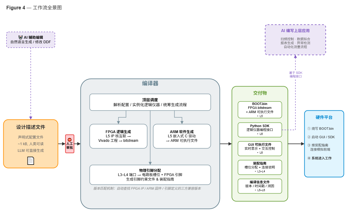
The compiler reads the configuration file and automatically transforms it into runnable hardware. Internally, it is organized into four layers:
- Top-level scheduler. Parses the configuration file, determines which functional blocks each logical instrument requires, and coordinates the subsequent generation stages.
- FPGA logic generation (corresponding to L5). Selects the digital signal processing functional blocks required by each logical instrument (e.g., the demodulation IP core of a lock-in amplifier, the waveform capture IP core of an oscilloscope), interconnects them according to the signal flow topology, generates a Vivado project script, and synthesizes the FPGA bitstream.
- ARM embedded software generation (corresponding to L5). Selects the embedded firmware functional blocks for each logical instrument, generates the corresponding C driver code, compiles it into an ARM executable, and handles command forwarding and data transfer between the logical instruments and the host computer.
- Physical pin assignment (corresponding to L3–L4). Selects the analog front-end and digital I/O functional blocks required by each logical instrument, maps their ports to the physical slots and FPGA pins on the circuit board, generating pin constraint files and a physical assembly guide. The user inserts the analog front-end modules into the specified slots according to this guide.
A version matching mechanism ensures that the three functional blocks composing each logical instrument — an FPGA IP core (L5), an ARM embedded firmware component (L5), and a circuit board pin definition (L3–L4) — are version-aligned. The compiler maintains an internal compatibility table. When a user specifies a logical instrument, the compiler automatically looks up and loads mutually compatible versions of these three functional blocks. This eliminates the tedious and error-prone task of manually managing version compatibility across hardware and firmware.
The compiler provides two essential guarantees:
- Zero hardware coding. The user writes no hardware description language (HDL) or low-level DSP code, and manages no SPI timing parameters or pin assignments.
- Rapid reconfiguration. Modifying the configuration file and recompiling produces a completely new physical instrument in minutes for a typical system.
3.4 Compiler output and deployment
Upon completion, the compiler produces the following deliverables:
- L5 firmware. FPGA configuration file (bitstream), ARM embedded executable, and BOOT.bin startup file.
- L6 host software. A Python SDK providing a programming interface for each logical instrument, and a GUI executable for real-time display and interactive control.
- L3, L4 Assembly guide. Module slot assignment diagram and connection instructions.
- Build information file. A record of compilation time, compiler version, and module versions for complete traceability.
The user then: write the BOOT.bin to hardware → launch the GUI or import the SDK → plug in ADC, DAC and analog front-end modules according to the assembly guide → the system is operational.
Furthermore, the Python SDK produced by the compiler provides a programming interface that enables AI-assisted application-layer development. A large language model can use the SDK to write host applications that perform frequency sweeps, data fitting, report generation, anomaly detection, and other complex non-real-time functions — extending the compiler-generated real-time instrument core into a complete automated measurement workflow.
4. AI Compatibility and Conversational Instrument Design
4.1 The configuration file as a controlled vocabulary
The expressive power of the configuration file derives from a controlled vocabulary:
- The instrument type vocabulary is fixed and finite. Currently around a dozen types (oscilloscope, lock-in amplifier, PID controller, DDS signal source, and several ADC/DAC variants; see §3.2 table).
- Parameter rules are explicit. Each instrument type has a pre-defined set of configurable parameters with defined ranges. For example, an oscilloscope can only configure "channel count" and "capture depth" — there is no open-ended or ambiguous parameter space.
- Port syntax is simple. Ports have only two directions:
inputandoutput. Connection statements have only one form: "output port → input port."
This vocabulary has a finite number of entries and a strict grammar. The consequence is significant: whether the designer is a human or an AI, the probability of producing a valid configuration file is high, the probability of producing an invalid one is low, and any error is immediately caught by the compiler with a specific correction hint.
This stands in sharp contrast to having a large language model directly generate hardware description code (such as Verilog or VHDL). The latter has a nearly infinite combination space, with complex syntax and timing constraints. Generating correct hardware code remains a difficult challenge for AI. In our system, the task presented to the language model is simplified to: select instrument types from the controlled vocabulary, fill in parameters, and declare connections — fundamentally a problem of selection and assembly from a finite set of options, not open-ended code creation.
4.2 The safe two-stage architecture
The system adopts a dual-safeguard architecture shared by human and AI users:
- The language model (or human) acts as the designer. Based on measurement requirements, it selects logical instruments from the controlled vocabulary and writes a configuration file.
- The compiler acts as the implementer and gatekeeper. It performs strict validation of the configuration file: whether instrument names exist, whether parameters are within bounds, whether port types match, and whether the connection topology is legal. Any configuration file that fails validation is rejected outright — no hardware configuration is generated. When rejection occurs, the compiler returns the specific error location and a correction suggestion.
The configuration file becomes a safety barrier between design and implementation. Whether the designer is human or AI, the same compilation and validation step must be passed. The language model cannot — through "hallucination" (producing a configuration that appears plausible but contains errors) — cause the hardware to execute incorrect operations. The compiler is the final, non-bypassable line of defense.
4.3 Conversational instrument design workflow
The architecture described above naturally supports a conversational instrument design process:
- The user describes measurement requirements in natural language (e.g., "I need to measure the impedance spectrum of a sample, frequency range 1 Hz to 100 kHz").
- The language model consults the logical instrument library (§3.2 table) and the parameter specifications of each instrument, and generates a configuration file.
- The compiler validates the configuration file. If it passes, the compiler produces the complete physical instrument, and the user can begin measurement.
- If validation fails (e.g., a parameter is out of range, or a port connection error exists), the compiler returns specific error information. The language model corrects the configuration file based on this feedback and resubmits, forming a closed-loop iteration — continuing until compilation succeeds and the instrument is ready.
Throughout this entire process, the user needs no knowledge of FPGA or ARM programming, nor any manual management of hardware pin assignments. The user's interaction with the system remains at two levels: describing requirements and receiving an instrument. All intermediate technical details are handled jointly by the language model and the compiler.
5. Proof of Concept: Impedance Measurement
5.1 Measurement principle and objective
Impedance spectroscopy is a fundamental technique in materials characterization, electrochemical analysis, and bioimpedance studies. The core principle is to apply a sinusoidal excitation signal of known frequency to a device under test, measure the current flowing through the device, and use a lock-in amplifier to demodulate the in-phase and quadrature components of the current signal. From these components, the magnitude and phase of the complex impedance are computed.
The measurement chain is as follows: a signal generator produces a sinusoidal excitation voltage, which is output through a DAC and applied across the device under test. A transimpedance amplifier (TIA) converts the current flowing through the device into a voltage, which is digitized by an ADC. A lock-in amplifier module performs quadrature demodulation on this voltage signal, yielding the in-phase and quadrature components.
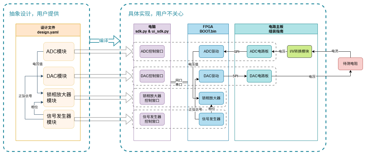
5.2 Designing the logical instrument configuration
For this measurement task, the user describes the requirements (or writes the configuration file directly), declaring the following logical instruments and their interconnections:
- Signal generator. Produces a frequency-adjustable sinusoidal excitation signal (0.1 Hz to 100 kHz), output through a DAC.
- Lock-in amplifier. Demodulates the current-channel signal, providing magnitude and phase outputs.
- ADC. Digitizes the conditioned current-channel signal (1 MSps, 20-bit) and feeds it to the lock-in amplifier.
- DAC. Outputs the excitation waveform (1 MSps, 20-bit).
The signal flow between logical instruments is:
Signal generator output → DAC → external analog front-end (exciting the device under test) → ADC captures current → Lock-in amplifier demodulates → Host computer computes impedance.
A corresponding excerpt of the design description file (instrument instances and port connections) is shown.
5.3 Compilation and physical assembly
The compiler reads the design description file and automatically:
- Validates logical instrument names, parameter ranges, and port type compatibility.
- Allocates physical modules: assigns transimpedance amplifier and output driver analog front-end modules, AD/DA modules, and maps FPGA pins and bus addresses.
- Generates the FPGA bitstream (pre-compiled lock-in amplifier and signal generator IP core netlists interconnected according to the signal flow), the Python SDK, and the GUI, and outputs the assembly guide.
The user follows the assembly guide to connect the L2 sensor ports (e.g., a four-terminal fixture) to the system, writes the bitstream, and launches the software.
5.4 Measurement results
- Impedance spectrum sweep. The GUI supports setting start frequency, stop frequency, and number of steps. It performs an automated frequency sweep, displaying impedance magnitude (|Z|) and phase (θ) curves as functions of frequency in real time.
- Single-frequency measurement. The user can select a fixed frequency for continuous measurement, displaying the complex impedance value.
- Workflow timing. The elapsed time from the design description to the first valid impedance spectrum is recorded (approximately 25 minutes in this case).
- Measured accuracy. Validated using a parallel network of standard resistors and capacitors, compared against a commercial impedance analyzer. Magnitude error is below 1%, phase error below 1° (below 100 kHz).
5.5 Reconfiguration into a different instrument
By modifying the design description file — adding a PID controller logical instrument alongside the existing signal generator — and recompiling, the system is transformed. The PID controller adjusts the signal generator's frequency parameter in the digital domain, locking the excitation frequency to the resonance of a mechanical resonator and maintaining resonant drive. The same hardware platform transitions from an impedance analyzer to a resonance frequency tracking driver in approximately 20 minutes.
Adding a second DAC output channel and routing the PID feedback signal to a laser tuning port (piezoelectric actuator or current modulation) reconfigures the system into a Pound-Drever-Hall (PDH) laser frequency stabilizer. At this point, the hardware platform simultaneously hosts signal generation, lock-in demodulation, PID control, and dual-channel DAC output on a single set of modular resources, demonstrating the core capability of the system: switching measurement paradigms through configuration changes alone. The current platform (ZYNQ7020 FPGA) supports approximately 10 logical instruments (ADCs and DACs excluded), depending on the type of logical instruments, and limited by FPGA logical resources.
6. Discussion
6.1 The logical instrument as a core abstraction
The logical instrument separates instrument specification from physical implementation. It serves as a common language for human-instrument interaction and AI-instrument interaction alike.
It is worth distinguishing the logical instrument from LabVIEW's "virtual instrument" concept. In LabVIEW, the user constructs a graphical dataflow diagram describing how instrument functionality is implemented — wiring together signal processing primitives. In our system, the user declares what instrument is needed (e.g., "one lock-in amplifier"), and the compiler generates its implementation. The logical instrument abstraction operates at the specification level; LabVIEW virtual instruments operate at the implementation level.
6.2 Limitations and future work
- Functional block library built from scratch. The current set of functional blocks is limited. Prioritizing coverage of high-demand measurement functions and establishing an open-source contribution mechanism are near-term needs.
- Performance ceiling. The system currently operates stably below the 100 MSps regime. Higher-speed L3 analog front-ends and tighter L5 integration are the next engineering challenges. The current L5 implementation uses FPGAs, but the logical instrument abstraction layer is independent of any specific processor architecture; as technology advances, the implementation can migrate to DSPs or other platforms.
- Multi-board synchronization. The current system is limited to a single board. Distributed multi-board measurement has not yet been implemented.
- Barrier to new functional block development. Creating a new functional block currently requires traditional HDL programming (for FPGA) or low-level DSP programming. Future work could provide high-level synthesis or model-based design interfaces to lower the barrier for third-party developers.
- Simulation based on logical instrument definitions. The inherent separation of specification from implementation in the logical instrument architecture means that the same design description can drive a simulator, producing a digital twin. This would enable rapid design verification without hardware and support AI training iterations. This is an important direction for future work.
- Long-term vision. Train a dedicated large model for scientific instrumentation that can not only compose existing functional blocks but also reason about the specifications of new functional blocks that are needed.
- Fully AI-driven physical experiments. The ultimate vision of this architecture is an "AI scientist": starting from an experimental hypothesis, an AI autonomously designs a measurement plan, generates the design description file, compiles and deploys the instrument, executes measurements, analyzes results, and iteratively adjusts experimental parameters or instrument configuration based on those results, forming a closed-loop automated scientific discovery process. The logical-instrument-plus-compiler two-stage architecture provides the safe engineering foundation for this: the AI's creative activity is confined to the design description layer and cannot compromise hardware safety.
6.3 Educational potential
Combined with a simulator, students could design and validate precision measurement systems in a zero-risk virtual environment, dramatically lowering the barrier to teaching instrumentation.
7. Conclusion
- We have constructed a reconfigurable instrument system centered on the logical instrument abstraction.
- Users define instrument systems through a declarative design description; a compiler produces the complete physical implementation within minutes.
- The six-layer reference model provides a precise analytical framework, and the horizontal packaging of functional blocks transforms instrument function from a permanently sealed enclosure into an open, composable set of building blocks.
- The design description file constitutes a finite controlled vocabulary, providing a solid foundation for safe AI-driven instrument design.
- The complete workflow has been validated: from natural language description to physical measurement, demonstrating the feasibility of a conversational, composable new era for instrumentation.
- Although the discussion centers on physics experiments, the same architecture applies equally to industrial measurement and control.